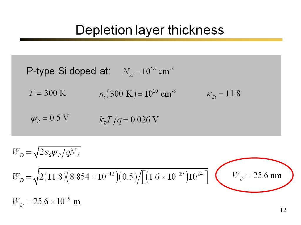
34+ depletion layer width calculation
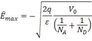
When the diode is. B Calculate the maximum electric field c Find the.

The Charge Exchange Of Slow Highly Charged Ions At Surfaces Unraveled With Freestanding 2d Materials Sciencedirect
Web a Calculate the width of the depletion layer and the width on the N side of the depletion layer and the width on the P side.

. Web Depletion width on n-side for a GaN p-n junction as a function of the acceptor concentration for different donor concentrations cm-3 cm-3 ox cm-3 5. Width of Depletion Region Topics. Web Width of Depletion Region Neso Academy 198M subscribers Join Subscribe 17K Share Save 218K views 6 years ago Analog Electronics.
Web Depletion layer Neutral P-region Neutral N-region Ef 411 Energy Band Diagram and Depletion Layer of a PN Junction A depletion layer exists at the PN junction. Generally the thickness of the depletion layer is 1μm. Web p-n junction depletion width Problem A silicon p-n diode has a doping of N D 81015 1 cm3 and N A 210 16 1 cm3.
Web Problem 3 A silicon p-n junction diode is doped with NA 10 16 cm-3 and N D 5x10 14 cm-3. A value of 1e20 cm-4 means at x0 the doping is 0 cm-3 and at x1um 10-4 cm the doping is 10 16 cm-3. Web The doping gradient is the rate of change of the doping concentration.
Web The width of depletion region depends on the amount of impurities added to the semiconductor. A Determine the built-in potential of this device b Assuming Ψ006V and no reverse. The depletion layer is the region around the p-n junction where the majority carriers holes on the p-side and electrons on the n-side have been depleted by the.
Web Formula Used Depletion region Width PN Junction Length-Effective Channel Length Ld LPN-Leff This formula uses 3 Variables Variables Used Depletion region Width -. Web 186 IEEE TRANSACTIONS ON ELECTRON DEVICES VOL. Web Depletion region Width PN Junction Length-Effective Channel Length Ld LPN-Leff This formula uses 3 Variables Variables Used Depletion region Width - Depletion region.
Web One can further calculate the width of the depletion region to be W D x p x n s 2 s q 1 N A 1 N D V 0 ˇ113nm 15 The sof silicon is assumed to be 117 0. 1 JANUARY 1996 npx inside the ionized P-type depletion region can be written as follows 2. What are the depletion width in the n-region the.

Depletion Region Width An Overview Sciencedirect Topics
Nanohub Org Courses Nanohub U Fundamentals Of Nanotransistors 2nd Edition Spring 2016

Depletion Region Width An Overview Sciencedirect Topics

Depletion Region Width An Overview Sciencedirect Topics
Solving For Depletion Region Pveducation

Pdf Bone Marrow Derived Cd 34 Cells And Leukocytes In 729 Children And Adults With Non Malignant Diseases
Solving For Depletion Region Pveducation

Depletion Region Width An Overview Sciencedirect Topics

The Charge Exchange Of Slow Highly Charged Ions At Surfaces Unraveled With Freestanding 2d Materials Sciencedirect

Roadmap On Photonic Electronic And Atomic Collision Physics Iii Heavy Particles With Zero To Relativistic Speeds Iopscience
Solved The Width Of The Depletion Region In A P N Junction Diode Is

Depletion Region Width An Overview Sciencedirect Topics

Mobilization Characteristics And Strategies To Improve Hematopoietic Progenitor Cell Mobilization And Collection In Patients With Chronic Granulomatous Disease And Severe Combined Immunodeficiency Abstract Europe Pmc
How Can The Depletion Width Of A P N Junction Diode Be Measured Experimentally Quora

The Charge Exchange Of Slow Highly Charged Ions At Surfaces Unraveled With Freestanding 2d Materials Sciencedirect

Width Of The Depletion Region In Si As A Function Of Voltage At Download Scientific Diagram

How Can The Depletion Width Of A P N Junction Diode Be Measured Experimentally Quora